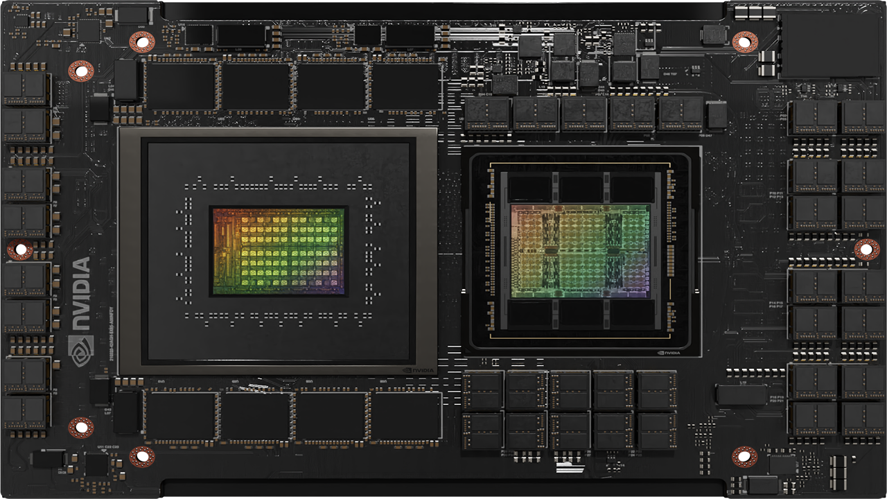
NVIDIA Grace CPU 是 NVIDIA 开发的第一个数据中心 CPU 。它是从头开始建造的,以创建 世界上第一个超级芯片 .
旨在提供卓越的性能和能效,以满足现代数据中心工作负载的供电需求 数字孪生 , 云游戏和图形 , 人工智能 和 高性能计算 ( HPC ) NVIDIA Grace CPU 具有 72 个 Armv9 GPU 内核,实现 Arm 可伸缩向量扩展第二版 ( SVE2 )指令集。核心还包括具有嵌套虚拟化功能和 S-EL2 支持的虚拟化扩展。
NVIDIA Grace CPU 还符合以下 Arm 规范:
- RAS v1.1 通用中断控制器( GIC ) v4.1
- 内存分区和监视( MPAM )
- 系统内存管理单元( SMMU ) v3.1
Grace CPU 被构建为与 NVIDIA Hopper GPU 创建用于大规模人工智能训练、推理和高性能计算的 NVIDIA Grace CPU 超级芯片,或与另一个 Grace CPU ,构建高性能[Z1K22],以满足高性能计算和云计算工作负载的需求。
继续阅读,了解 Grace CPU 的主要功能。
使用 NVLink-C2C 的高速芯片间互连
Grace Hopper 和 Grace 超级芯片均由 NVIDIA NVLink-C2C 高速芯片间互连,用作超级芯片通信的主干。
NVLink-C2C 扩展 NVIDIA NVLink 用于连接服务器中的多个 GPU ,以及使用 NVLink 交换机系统连接多个 GPU 节点。
NVLink-C2C 在封装上的裸片之间具有 900GB / s 的原始双向带宽,提供了 PCIe Gen 5 x16 链路的 7 倍带宽(与使用 NVLink 时 NVIDIA Hopper GPU 之间可用的带宽相同)和更低的延迟。 NVLink-C2C 还只需要传输 1.3 微微焦耳/位,这是 PCIe Gen 5 能效的 5 倍以上。
NVLink-C2C 也是一种相干互连,在使用 Grace CPU 超级芯片对标准相干[Z1K22]平台以及使用 Grace Hopper 超级芯片的异构编程模型进行编程时,能够实现一致性。
使用 NVIDIA Grace CPU 的符合标准的平台
NVIDIA Grace CPU 超级芯片旨在为软件开发人员提供符合标准的平台。 Arm 提供了一套规范,作为其系统就绪计划的一部分,旨在为 Arm 生态系统带来标准化。
Grace CPU 以 Arm 系统标准为目标,提供与现成操作系统和软件应用程序的兼容性, Grace CPU 将从一开始就利用 NVIDIA Arm 软件堆栈。
Grace CPU 还符合 Arm 服务器基础系统架构( SBSA ),以实现符合标准的硬件和软件接口。此外,为了在基于 Grace CPU 的系统上启用标准引导流, Grace CPU 被设计为支持 Arm 服务器基本引导要求( SBBR )。
对于缓存和带宽分区以及带宽监控, Grace CPU 还支持 Arm 内存分区和监控( MPAM )。
Grace CPU 还包括 Arm 性能监控单元,允许对 GPU 内核以及片上系统( SoC )架构中的其他子系统进行性能监控。这使得标准工具(如 Linux perf )可以用于性能调查。
带 Grace Hopper 超级芯片的统一内存
NVIDIA Grace Hopper 超级芯片将 Grace CPU 与 Hopper GPU 相结合,扩展了 CUDA 在 CUDA 8.0 中首次引入的统一内存编程模型。
NVIDIA Grace Hopper 超级芯片引入了具有共享页表的统一内存,允许 Grace CPU 和 Hopper GPU 与 CUDA 应用程序共享地址空间甚至页表。
Grace Hopper GPU 还可以访问可分页内存分配。 Grace Hopper 超级芯片允许程序员使用系统分配器分配 GPU 内存,包括与 GPU 交换指向malloc内存的指针。
NVLink-C2C 支持 Grace CPU 和 Hopper GPU 之间的本机原子支持,释放了 CUDA 10.2 中首次引入的 C ++原子的全部潜力。
NVIDIA 可伸缩一致性结构
Grace CPU 介绍了 NVIDIA 可伸缩一致性结构( SCF )。由 NVIDIA 设计的 SCF 是一种网格结构和分布式缓存,旨在根据数据中心的需要进行扩展。 SCF 提供 3.2 TB / s 的二等分带宽,以确保 NVLink-C2C 、 CPU 核心、内存和系统 IO 之间的数据流量。
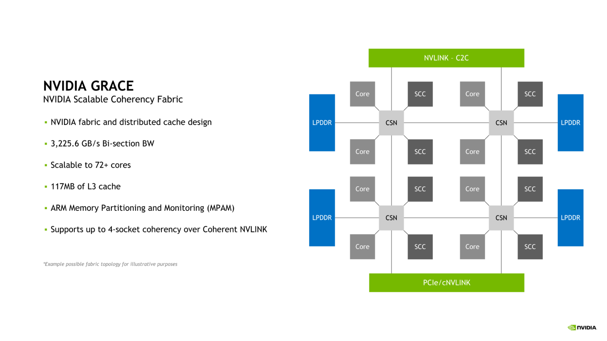
单个 Grace CPU 包含 72 个 GPU 内核和 117MB 缓存,但 SCF 的设计可扩展性超出此配置。当两个 Grace CPU 组合形成一个 Grace 超级芯片时,这些数字分别增加到 144 个 CPU 核和 234MB 的 L3 缓存。
CPU 核心和 SCF 缓存分区( SCC )分布在整个网格中。缓存交换节点( CSN )通过结构路由数据,并充当 CPU 核心、缓存内存和系统其余部分之间的接口,从而实现整个系统的高带宽。
内存分区和监视
Grace CPU 集成了对内存系统资源分区和监控( MPAM )功能的支持,这是 Arm 对系统缓存和内存资源进行分区的标准。
MPAM 通过向系统内的请求者分配分区 ID ( PartID )来工作。这种设计允许基于其各自的分区对资源(如缓存容量和内存带宽)进行分区或监控。
Grace CPU 中的 SCF 缓存支持使用 MPAM 对缓存容量和内存带宽进行分区。此外,性能监视组( PMG )可用于监视资源使用情况。
利用内存子系统提高带宽和能效
为了提供卓越的带宽和能效, Grace CPU 实现了 32 通道 LPDDR5X 内存接口。这提供了高达 512GB 的内存容量和高达 546GB / s 的内存带宽。
扩展 GPU 存储器
Grace Hopper 超级芯片的一个关键特征是引入了扩展 GPU 内存( EGM )。通过允许从更大的 NVLink 网络连接的任何漏斗 GPU 访问连接到 Grace Hopper 超级芯片中 Grace CPU 的 LPDDR5X 内存,大大扩展了 GPU 可用的内存池。
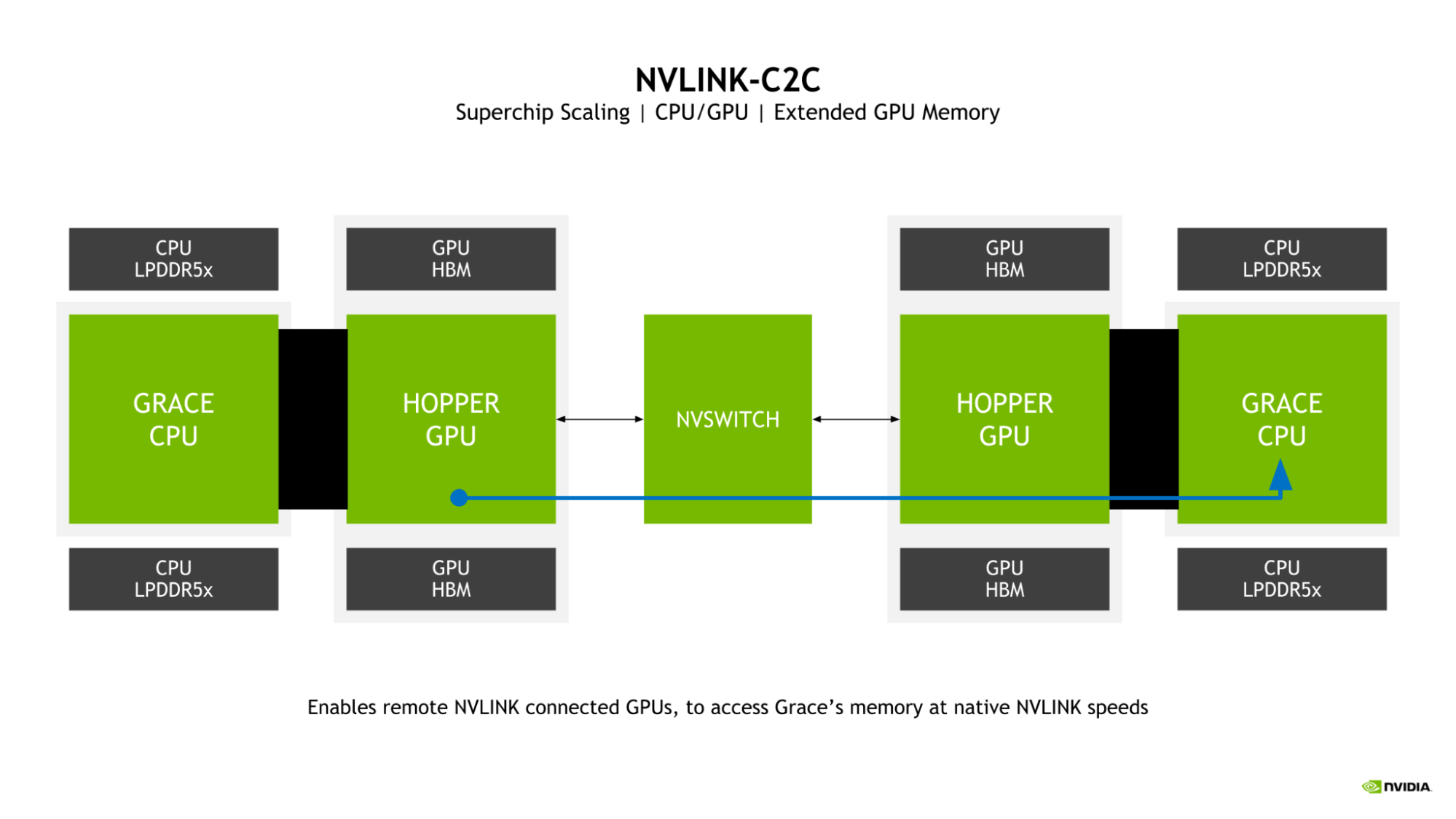
GPU 到 – GPU NVLink 和 NVLink-C2C 双向带宽在超级芯片中匹配,这使得料斗 GPU 能够以 NVLink 本地速度访问 Grace CPU 存储器。
使用 LPDDR5X 平衡带宽和能效
为 Grace CPU 选择 LPDDR5X 是因为需要在大规模 AI 和 HPC 工作负载的带宽、能效、容量和成本之间取得最佳平衡。
虽然四站点 HBM2e 内存子系统将提供大量内存带宽和良好的能效,但其成本将是 DDR5 或 LPDDR5X 每 GB 成本的 3 倍以上。
此外,这种配置将仅限于 64GB 的容量,这是具有 LPDDR5X 的 Grace CPU 可用的最大容量的八分之一。
与更传统的八通道 DDR5 设计相比, Grace CPU LPDDR5X 内存子系统提供了高达 53% 的带宽,并大大提高了功率效率,每千兆字节只需要八分之一的功率。
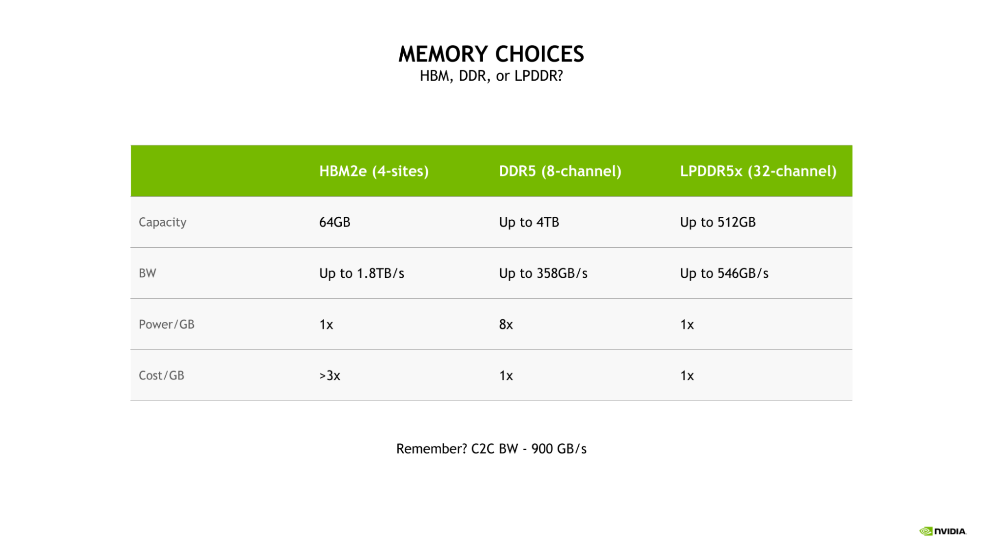
LPDDR5X 卓越的功率效率使得能够将更多的总功率预算分配给计算资源,例如 CPU 核或 GPU 流式多处理器( SMs )。
NVIDIA Grace CPU 输入/输出
Grace CPU 整合了一系列高速 I / O ,以满足现代数据中心的需求。 Grace CPU SoC 提供多达 68 条 PCIe 连接通道和多达 4 条 PCIe Gen 5 x16 链路。每个 PCIe Gen 5 x16 链路提供高达 128GB / s 的双向带宽,并可进一步分叉为两个 PCIe Gen 5×8 链路,以实现额外的连接。
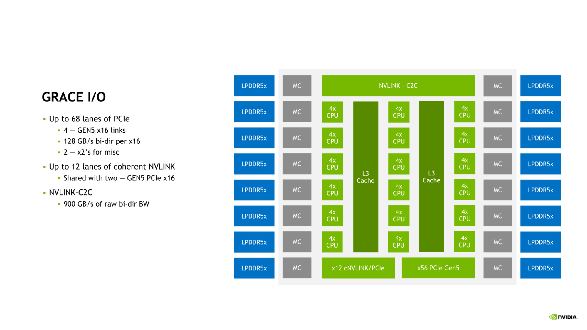
这种连接是对片上 NVLink-C2C 链路的补充,该链路可用于将 Grace CPU 连接到另一个 Grace CPU ,或连接到 NVIDIA Hopper GPU 。
NVLink 、 NVLink-C2C 和 PCIe Gen 5 的组合为 Grace CPU 提供了丰富的连接选项套件和扩展现代数据中心性能所需的充足带宽。
NVIDIA Grace CPU 性能
NVIDIA Grace CPU 设计用于在单芯片和 Grace 超级芯片配置中提供卓越的计算性能,估计SPECrate2017_int_base得分分别为 370 和 740 。这些预硅估计基于 GNU 编译器集合( GCC )的使用。

内存带宽对于设计 Grace CPU 的工作负载至关重要,在流基准测试中,单个 Grace CPU ,预计可提供高达 536GB / s 的实际带宽,占芯片峰值理论带宽的 98% 以上。

最后,料斗 GPU 和 Grace CPU 之间的带宽对于最大化 Grace 料斗超级芯片的性能至关重要。 GPU 对 – CPU 内存的读和写预计分别为 429GB / s 和 407GB / s ,分别代表 NVLink-C2C 峰值理论单向传输速率的 95% 和 90% 以上。
综合读写性能预计为 506GB / s ,占单个 NVIDIA Grace CPU SoC 可用峰值理论内存带宽的 92% 以上。

NVIDIA Grace CPU 超级芯片的优势
NVIDIA Grace CPU 超级芯片拥有 144 个核心和 1TB / s 的内存带宽,将为基于 CPU 的高性能计算应用提供前所未有的性能。 HPC 应用程序是计算密集型应用程序,需要性能最高的核心、最高的内存带宽和每个核心的正确内存容量,以加快结果。
NVIDIA 正在与领先的 HPC 、超级计算、超尺度和云客户合作,开发 Grace CPU 超级芯片。 Grace CPU 超级芯片和 Grace Hopper 超级芯片预计将于 2023 年上半年上市。
有关 NVIDIA Grace Hopper 超级芯片和 NVIDIA Grace CPU 超级芯片的更多信息,请访问 NVIDIA Grace CPU .