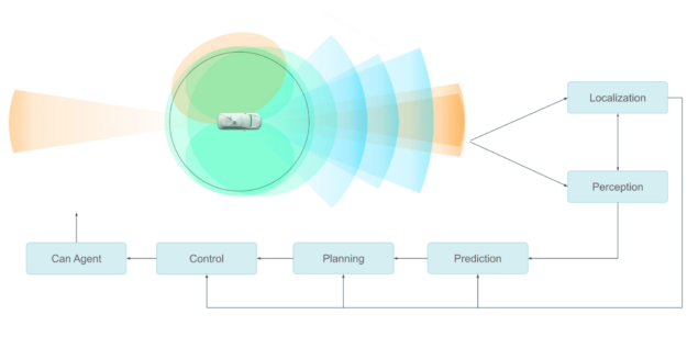
就像人类依靠眼睛看东西一样,自动驾驶汽车使用传感器收集信息。这些传感器收集大量数据,这需要高效的车载数据处理,以便车辆对道路上的情况做出快速反应。这种能力对于自动驾驶汽车的安全至关重要,对于让虚拟驾驶员更智能也至关重要。
由于需要冗余和多样的传感器和计算系统,设计和优化处理管道是一项挑战。在这篇文章中,我们将介绍Pony.ai 的演变。人工智能的车载传感器数据处理管道。
Pony.ai 能的传感器设置包括多个摄像头、激光雷达和雷达。上游模块同步传感器,将数据封装成消息片段,并将其发送给下游模块,这些模块使用它们来分割、分类和检测对象,等等
每种类型的传感器数据可能有多个模块,用户算法可以是传统的,也可以是基于神经网络的。
整个管道必须以最高的效率运行。乘客的安全是我们的首要任务。传感器数据处理系统在两个方面影响安全。
首先,安全性的决定因素之一是自动驾驶系统处理传感器数据的速度。如果感知和定位算法以数百毫秒的延迟获得传感器数据,那么车辆做出的决定就太晚了。
第二,整个硬件/软件系统必须可靠,才能长期成功。如果自动驾驶汽车在制造几个月后开始出现问题,消费者将永远不会想要购买或乘坐该车。这在大规模生产阶段至关重要。
高效处理传感器数据
缓解传感器处理管道中的瓶颈需要采用多方面的方法,同时考虑传感器、 GPU 体系结构和 GPU 内存。
从传感器到 GPU
当 Pony.ai 成立时,我们最初的传感器设置由现成的组件组成。我们为摄像头使用了基于 USB 和以太网的型号,摄像头直接连接到车载计算机, CPU 负责从 USB /以太网接口读取数据。
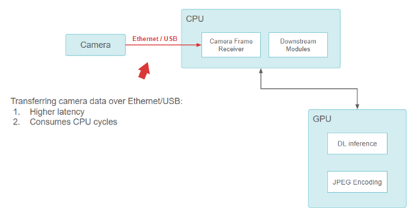
通过以太网/ USB 传输摄像头数据提供了更高的延迟,但需要 CPU 个周期。
虽然功能良好,但设计存在一个根本问题。 USB 和以太网摄像头接口( GigE 摄像头)占用 CPU 。随着越来越多的高分辨率摄像头的加入, CPU 很快变得不知所措,无法执行所有的 I / O 操作。这种设计很难在保持足够低的延迟的同时实现可扩展性。
我们通过为摄像头和激光雷达添加基于 FPGA 的传感器网关解决了这个问题。
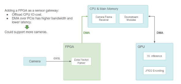
添加 FPGA 作为传感器网关 可以降低 CPU I / O 成本,但 PCIe 上的 DMA 具有更高的带宽和更低的延迟,因此它可以支持更多摄像头。
FPGA 处理摄像头触发和同步逻辑,以提供更好的传感器融合。当一个或多个摄像头数据包准备就绪时,触发 DMA 传输,以通过 PCIe 总线将数据从 FPGA 复制到主存储器。 DMA 引擎在 FPGA 上执行此操作, CPU 被释放。它不仅可以打开 CPU 的 I / O 资源,还可以减少数据传输延迟,从而实现更具可扩展性的传感器设置。
由于在 GPU 上运行的许多神经网络模型都使用相机数据,因此在通过 DMA 将其从 FPGA 传输到 CPU 后,仍然必须将其复制到 GPU 内存中。因此,某个地方需要 CUDA HostToDevice内存拷贝, FHD 相机图像的单帧需要约 1.5 毫秒。
然而,我们希望进一步减少这种延迟。理想情况下,摄像机数据应直接传输到 GPU 内存中,而无需通过 CPU 路由。
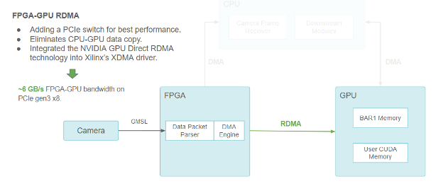
使用 FPGA- GPU RDMA ,我们添加了一个 PCIe 交换机以获得最佳性能。该解决方案消除了 CPU- GPU 数据拷贝。我们还将 NVIDIA GPU 直接 RDMA 技术集成到 Xilinx 的 XDMA 驱动程序中,在 PCIe Gen3 x8 上提供约 6 GB / s 的 FPGA- GPU 带宽。
我们通过使用 NVIDIA GPU 直接 RDMA 实现了这一目标。 GPU 直接 RDMA 使我们能够通过 PCIe 条(定义 PCIe 地址空间线性窗口的基址寄存器)预先分配可供 PCIe 对等方访问的 CUDA 内存块。
它还为第三方设备驱动程序提供了一系列内核空间 API ,以获取 GPU 内存物理地址。这些 API 有助于第三方设备中的 DMA 引擎直接向 GPU 内存发送和读取数据,就像它向主存发送和读取数据一样。
GPU 直接 RDMA 通过消除 CPU 到 – GPU 拷贝来减少延迟,并在 PCIe Gen3 x8 下实现最高带宽~ 6 GB / s ,其理论限制为 8 GB / s 。
跨 GPU 缩放
由于计算工作量的增加,我们需要不止一个 GPU 。随着越来越多的 GPU 添加到系统中, GPU 之间的通信也可能成为瓶颈。通过暂存缓冲区通过 CPU 会增加 CPU 成本并限制总体带宽。
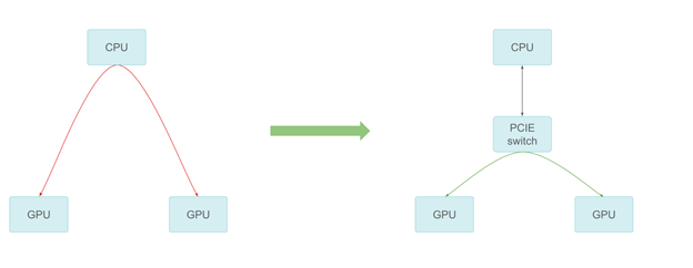
我们添加了一个 PCIe 交换机,它提供了尽可能最好的对等传输性能。在我们的测量中,对等通信可以达到 PCIe 线速度,从而在多个 GPU 之间提供更好的可扩展性。
将计算转移到专用硬件
我们还将以前在 CUDA 内核上运行的任务卸载到专用硬件上,以加速传感器数据处理。
例如,将 FHD 摄像头图像编码为 JPEG 字符串时, NvJPEG 库在带有 RTX5000 GPU 的单个 CPU 线程上需要约 4ms 的时间。 NvJPEG 可能会消耗 CPU 和 GPU 资源,因为它的某些阶段,比如哈夫曼编码,可能完全在 CPU 上。
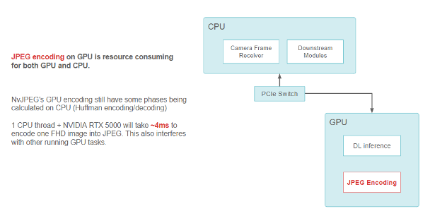
GPU 上的 JPEG 编码会消耗 GPU 和 CPU 的资源。 NvJPEG GPU 编码仍有一些相位在 CPU 上计算(哈夫曼编码和解码)。一个 CPU 线程加上 NVIDIA RTX 5000 需要约 4ms 才能将一幅 FHD 图像编码为 JPEG 。这也会干扰其他正在运行的 GPU 任务。
我们采用 NVIDIA 车载视频编解码器来减轻 CPU 和 GPU ( CUDA 部分)进行图像编码和解码的负担。该编解码器在 GPU 的专用部分使用编码器。它是 GPU 的一部分,但与用于运行内核和深度学习模型的其他 CUDA 资源不冲突。
我们还通过使用 NVIDIA GPU 上的专用硬件视频编码器,将图像压缩格式从 JPEG 迁移到了 HEVC ( H.265 )。我们实现了编码速度的提高,并将 CPU 和 GPU 资源释放出来用于其他任务。
在 GPU 上完全编码 FHD 图像需要约 3 毫秒,而不会影响其 CUDA 性能。性能是在仅 I 帧模式下测量的,这确保了帧间一致的质量和压缩伪影。
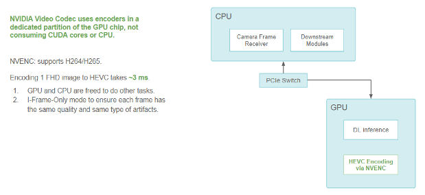
NVIDIA 视频编解码器在 GPU 芯片的专用分区中使用编码器,不消耗 CUDA 内核或 CPU 。 NVENC 支持 H264 / H265 。将一幅 FHD 图像编码到 HEVC 需要约 3 毫秒,因此 GPU 和 CPU 可以自由地执行其他任务。我们使用 I-frame-only 模式来确保每个帧具有相同的质量和相同类型的工件。
关于 – GPU 数据流
另一个关键主题是将相机帧作为消息发送到下游模块的效率。
我们使用谷歌的 protobuf 来定义一条消息。以CameraFrame消息为例。相机规格和属性是消息中的基本类型。由于 protobuf 的限制,实际有效载荷摄像头数据必须定义为主系统内存中的字节字段。
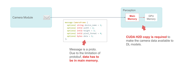
下面代码示例中的消息是 proto 。由于protobuf的限制,数据必须在主存中。
message CameraFrame {
 optional string device_name = 1;
 optional int32 width = 2;
 optional int32 height = 3;
 optional int32 pixel_format = 4;
 optional bytes data = 5;
};
需要 CUDA H2D 副本,才能使 DL 型号获得摄像头数据。
我们使用发布者 – 订阅者模型,在模块之间传递零拷贝消息以共享信息。此CameraFrame消息的许多订户模块使用摄像头数据进行深入学习推断。
在最初的设计中,当这样的模块收到消息时,它必须调用 CUDA HostToDevice内存副本,以便在推断之前将相机数据传输到 GPU 。
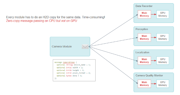
每个模块都必须对相同的数据进行 H2D 复制,这很耗时!下面的代码示例显示在 CPU 上传递的零拷贝消息,但不在 GPU 上传递。
message CameraFrame {
 optional string device_name = 1;
 optional int32 width = 2;
 optional int32 height = 3;
 optional int32 pixel_format = 4;
 optional bytes data = 5;
};
每个模块都必须进行 CUDA HostToDevice复制,这是冗余的,而且会消耗资源。尽管零拷贝消息传递框架在 CPU 上运行良好,但它涉及大量 CPU- GPU 数据拷贝。

我们使用 protobuf codegen插件来启用 GPU 内存中的数据字段。下面的代码示例显示了在 GPU 上传递的零拷贝消息。GPUData字段位于 GPU 内存中。
message CameraFrame {
 optional string device_name = 1;
 optional int32 width = 2;
 optional int32 height = 3;
 optional int32 pixel_format = 4;
 optional GpuData data = 5;
};
我们通过 protobuf 的插件 API 向 protobuf 代码生成器中添加了一种新类型的数据GpuData字段,从而解决了这个问题。GpuData支持标准的resize操作,就像 CPU 内存bytes字段一样。然而,它的物理数据存储在 GPU 上。
当用户模块收到消息时,它们可以检索 GPU 数据指针以供直接使用。因此,我们在整个管道中实现了完全零拷贝。
改进 GPU 内存分配
当我们调用GpuData原型的resize函数时,它调用 CUDA cudaMalloc。当GpuData原型消息被销毁时,它会调用cudaFree。
这两个 API 操作并不便宜,因为它们必须修改 GPU 的内存映射。每次通话可能需要约 0.1 毫秒。
由于在摄像机不间断地生成数据时,该协议被广泛使用,因此我们应该优化 GPU 协议的alloc/free成本。
我们实现了一个固定插槽大小的 GPU 内存来解决这个问题。想法很简单:我们维护一堆预先分配的 GPU 内存插槽,这些插槽与我们想要的相机数据帧缓冲区大小相匹配。每次调用alloc时,我们从堆栈中取出一个插槽。每次调用free时,插槽都会返回到池中。通过重新使用 GPU 内存,alloc/free时间接近于零。
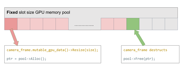
camera_frame.mutable_gpu_data()->Resize(size);
ptr = pool->Alloc();
如果我们想支持不同分辨率的摄像头呢?使用这个固定大小的内存池,我们必须始终分配最大的内存池大小,或者使用不同的插槽大小初始化多个内存池。两者都会降低效率。
CUDA 11.2 中的新功能解决了这个问题。它正式支持cudaMemPool,可以预先分配,然后用于cudaMalloc和free。与我们之前的实现相比,它有助于任何分配大小。这大大提高了灵活性,但性能成本很低(每次分配约 2 个)。
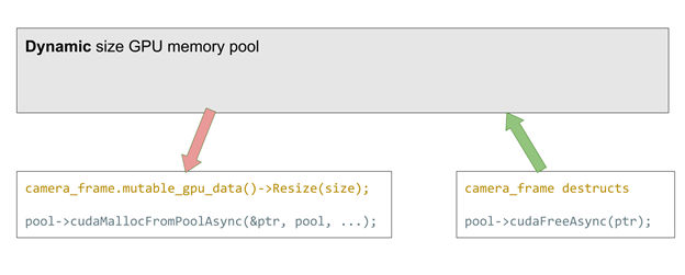
camera_frame.mutable_gpu_data()->Resize(size);
pool->cudaMallocFromPoolAsync(&ptr, pool, ...);
在这两种方法中,当内存池溢出时,resize调用会返回到传统的cudaMalloc和free。
YUV 颜色空间中更干净的数据流
通过之前对硬件设计和系统软件架构的所有优化,我们实现了高效的数据流。下一步是优化数据格式本身。
我们的系统用于在 RGB 颜色空间中处理相机数据。然而,我们相机的 ISP 输出在 YUV 颜色空间中,并且在 GPU 上执行从 YUV 到 RGB 的转换,这需要约 0.3 毫秒。此外,一些感知组件不需要颜色信息。向它们提供 RGB 颜色像素是浪费。
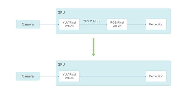
由于这些原因,我们从 RGB 相机帧迁移到 YUV 帧。我们选择使用 YUV420 像素格式,因为人类视觉对色度信息的敏感度不如对亮度信息的敏感度。
通过采用 YUV420 像素格式,我们节省了 GPU 内存消耗的一半。这也使我们能够仅向感知组件发送 Y 通道,感知组件不需要色度信息,与 RGB 相比,节省了 GPU 内存消耗的三分之二。
在 GPU 上处理激光雷达数据
除了相机数据,我们还处理激光雷达数据,这是更稀疏的,主要是在 GPU 上。考虑到不同类型的激光雷达,处理起来更困难。我们在处理激光雷达数据时进行了几次优化:
- 由于激光雷达扫描数据包含大量的物理信息,我们使用 GPU 友好的阵列结构而不是结构阵列来描述点云,使 GPU 内存访问模式更紧密而不是分散。
- 当一些字段必须在 CPU 和 GPU 之间交换时,我们将它们保存在页面锁定内存中,以加速传输。
- NVIDIA CUB 库广泛用于我们的处理管道,特别是扫描/选择操作。
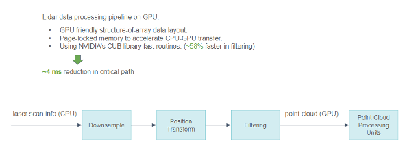
GPU 上的激光雷达数据处理管道产生以下结果:
- 一种 GPU 友好的阵列数据布局结构。
- 页面锁定内存以加速 CPU- GPU 传输。
- NVIDIA CUB 库快速例程,过滤速度快约 58% 。
通过所有这些优化,我们在关键路径中将整个管道延迟减少了约 4 毫秒。
总体时间表
通过所有这些优化,我们可以使用内部时间线可视化工具查看系统跟踪。
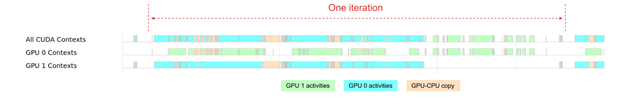
总体时间线显示了我们今天对 GPU 的依赖程度。虽然这两个 GPU 在大约 80% 的时间内都在使用,但 GPU0 和 GPU1 的工作负载并不理想。对于 GPU 0 ,它在整个 perception module 迭代中被大量使用。对于 GPU 1 ,它在迭代的中间有更多的空闲间隙。
未来,我们将专注于进一步提高 GPU 效率。
生产准备
在开发的早期, FPGA 使我们能够轻松地在基于硬件的传感器数据处理中试验我们的想法。随着我们的传感器数据处理器变得越来越成熟,我们一直在研究使用片上系统( SoC )来提供紧凑、可靠、可生产的传感器数据处理器的可能性。
我们发现汽车级 NVIDIA DRIVE Orin SoC 完全符合我们的要求。它是 ASIL 等级,非常适合在生产车辆上运行。
从 FPGA 迁移到 NVIDIA DRIVE Orin
在开发的早期, FPGA 使我们能够轻松地在基于硬件的传感器数据处理中试验我们的想法。
随着我们的传感器数据处理器变得越来越成熟,我们一直在研究使用片上系统( SoC )来提供紧凑、可靠、可生产的传感器数据处理器的可能性。
我们发现汽车级 NVIDIA DRIVE Orin SoC 完全符合我们的要求。它是 ASIL 等级,非常适合在生产车辆上运行。尽管其体积小、成本低,但它可以连接到各种汽车级传感器,并有效地处理大规模传感器数据。
我们将使用 NVIDIA Orin 来处理所有传感器信号处理、同步、数据包收集以及相机帧编码。我们估计,这种设计,结合其他架构优化,将节省约 70% 的 BOM 总成本。
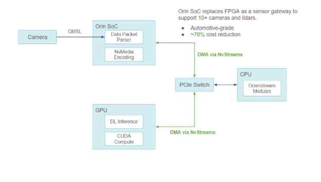
Orin SoC 取代 FPGA 作为传感器网关,支持 10 多个摄像头和激光雷达,这是汽车级的,成本降低约 70% 。
在与 NVIDIA 的合作中,我们确保 Orin CPU- GPU 组件之间的所有通信都通过 PCIe 总线,并通过 NvStreams 支持 DMA 。
- 对于计算密集型 DL 工作, NVIDIA Orin SoC 使用 NvStream 将传感器数据传输到离散的 GPU 进行处理。
- 对于非 GPU 工作, NVIDIA Orin SoC 使用 NvStream 将数据传输到主机 CPU 进行处理。
2 / 3 级计算平台应用程序
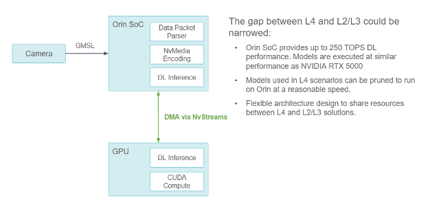
L4 和 L2 / L3 之间的差距可以缩小,因为 Orin SoC 提供高达 250 个顶级 DL 性能。模型的执行性能与 NVIDIA RTX 5000 类似,因此 L4 场景中使用的模型可以被删减,以合理的速度在 Orin 上运行。灵活的体系结构设计可以在 L4 和 L2 / L3 解决方案之间共享资源。
这种设计的一个显著优点是,它有潜力被用作 L2 / L3 计算平台。
NVIDIA Orin 每秒提供 254 万亿次运算,其计算能力可能与我们目前的 4 级自主车辆计算平台上使用的 RTX5000 离散式 GPU 类似。然而,要充分发挥 NVIDIA Orin SoC 的潜力,需要进行多项优化,例如:
- 结构稀疏网络
- 对于核心
- 跨多个 NVIDIA Orin SOC 扩展
结论
Pony 传感器数据处理管道的演变证明了我们朝着高效数据处理管道和增强系统可靠性的方向发展的系统方法,这有助于实现更高的安全目标。这种方法背后的简单想法是:
- 使数据流简单流畅。数据应该以最小化转换开销的格式直接传输到将被使用的位置。
- 为计算密集型任务使用专用硬件,并为其他任务节省通用计算资源。
- 4 级和 2 级系统之间的资源共享提高了可靠性并节省了工程成本。
硬件和软件不能单独通过共同努力来实现。我们认为,这对于满足快速增长的计算需求和生产预期至关重要。
致谢
这篇文章包括 Pony.ai 传感器数据管道多年的发展。这项荣誉属于多个团队和工程师,他们一直在为开发这种高效的传感器数据管道做出贡献。